Fast burst of infrared light opens a way for 3D processing inside semiconductor chips
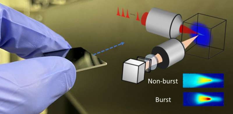
Researchers from LP3 Laboratory in France developed a light-based technique for local material processing anywhere in the three-dimensional space of semiconductor chips. The direct laser writing of new functionalities opens the possibility to exploit the sub-surface space for higher integration densities and extra functions.

Semiconductors remain the backbone material of the electronics integrated with modern devices such as cellphones, cars, robots and many other intelligent devices. Driven by the continuous need for miniaturized and powerful chips, the current semiconductor manufacturing technologies are facing increasing pressure.
The dominating manufacturing technology, lithography, has strong limitations when addressing these challenges, given its surface processing nature. For this reason, a solution to fabricating structures under the wafer surfaces would be highly desirable so that the full space inside the materials could be exploited.
Publishing their report in the International Journal of Extreme Manufacturing, the LP3 researchers demonstrate the fabrication of embedded structures inside various semiconductor materials, including Si and GaAs—two important materials for the microelectronics industry which cannot be 3D processed with conventional ultrafast lasers.
The first requirement is the right choice of wavelength so that the light can penetrate the semiconductor material. In this research, the wavelength used is in the infrared, very similar to that used for telecommunication applications, so that the semiconductors are a fully transparent material.
Framed by the European Horizon project "Extreme-Light Seeded Control of Ultrafast Laser Material Modifications," the team have made continuous efforts to extend the current spectrum of laser processing to a wider range from UV to infrared and even longer wavelengths. In this research, the standard telecommunication or so-called SWIR wavelengths were rapidly identified as excellent candidates for 3D processing inside semiconductors.
Although the technical issue of the appropriate wavelength was solved, there are some other physical limitations to tackle. With the use of intense light, as required for material processing, highly efficient nonlinear ionization inside narrow gap materials creates free electrons inside the material. This will rapidly transform any semiconductor into metal-like materials, which makes it impossible to propagate light deep inside the matter. This transition deteriorates the focusing process and prevents the occurrence of material modification using ultrafast lasers.
To solve this problem, the team proposed using non-conventional ultrafast bursts of pulses to circumvent the metallization transition. Explaining this, Dr. Andong Wang, one of the main investigators of this paper, says, "Previous research used too strong light pulses that were exciting the electrons too easily. Here, instead of using strong light pulses, we split the pulse energy into a large number of weaker pulses with an extremely fast repetition rate. These pulse trains, also named bursts, will avoid strong pulse excitation before the light is focused. Additionally, the pulses will repeat very fast so that the delivered laser energy can accumulate efficiently to cross the modification."
The team leader behind this work, Dr. David Grojo, says, "This offers the first very practical solution for ultrafast laser writing inside semiconductors. The next step will be to concentrate on the type of modifications that can be achieved inside these materials. Refractive index engineering is surely an important target given the growing importance of silicon photonics. Laser writing would offer the possibility of direct digital fabrication of 3D architecture materials inaccessible by current manufacturing technologies. In the future, these new laser modalities may drastically change the way advanced micro-chips are today fabricated."


