Technique simultaneously locates multiple defects on microchip circuits
Defective computer chips are the bane of the semiconductor industry. Even a seemingly minor flaw in a chip packed with billions of electrical connections might cause a critical operation in a computer or other sensitive electronic device to fail.
By modifying an existing technique for identifying defects, researchers at the National Institute of Standards and Technology (NIST) have developed a method that can simultaneously locate individual electrical flaws in multiple microcircuits on the same chip. Because the technique relies on a relatively inexpensive and common imaging tool, an atomic force microscope (AFM), it may provide a new way to test the interconnected wiring of computer chips in the factory.
An AFM features an ultrasharp tip attached to a tiny cantilever that vibrates like a diving board. In the standard mode of operation, scientists apply an AC (alternating current) voltage to the tip as it scans across individual wires buried in parallel several micrometers (millionths of a meter) below the surface of a silicon chip. The voltage difference between the tip and each wire generates an electric force revealed as changes in the frequency or amplitude (height) of the vibrating tip. A break or defect in a wire will show up as an abrupt change in the vibration of the tip.
However, that method of searching for defects with an AFM, known as electrostatic force microscopy (EFM), has a drawback. The vibration of the tip is affected not only by the static electric field from the wire under study but also by the voltages from all the neighboring wires. Those extraneous signals interfere with the ability to clearly image defects in the wire undergoing scanning.
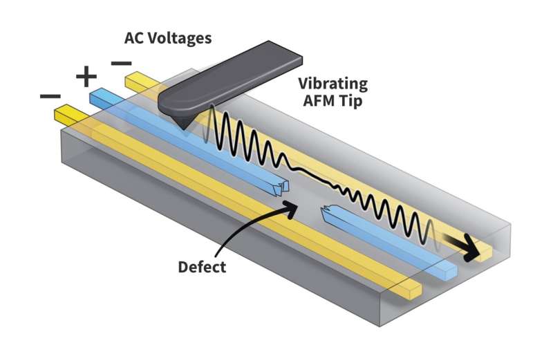
NIST scientists Joseph Kopanski, Evgheni Strelcov and Lin You solved the problem by applying specific AC voltages, supplied by an external generator, to individual neighboring wires instead of to the tip. An AC voltage alternates between positive and negative values; traced over time the voltage resembles a wave with peaks and valleys. In a single cycle, the voltage reaches its maximum positive voltage (the peak) and then falls to its lowest negative voltage (the valley).

Out-of-phase AC voltages (indicated by plus and minus) are applied to neighboring wires. A defect shows up as a clear change in the vibration of the tip as it is moved along the wire. Credit: S. Kelley/NIST
Taking advantage of this cyclic nature, the researchers applied the same AC voltage to neighboring wires as they did to the wire undergoing scanning, with one important difference: The voltages to the neighbors were exactly out of phase. Whenever the voltage to the wire of interest reached its highest value, the voltages to the neighboring wires were at their lowest.
The out-of-phase voltages exerted electrostatic forces on the AFM tip that opposed the force exerted by the scanned wire. Those oppositely directed forces translated into regions of high contrast on an AFM image, making it easier to distinguish the signal from the wire of interest.
Using a test chip featuring four pairs of wires buried 4 micrometers beneath the surface, the scientists demonstrated that their technique produced clear and accurate images of defects. And in tailoring the AC voltages applied to each wire so that they have different frequencies, the researchers showed that they could image defects in several adjacent wires at the same time.
Because the technique depends on an AC voltage applied remotely, to the wires rather than the AFM, the researchers have dubbed the technique remote bias-induced electrostatic force microscopy.
"Applying a voltage to the wires instead of the AFM tip may seem like a small innovation, but it makes a big difference," Kopanski said. "The method does not require a new instrument and could be easily implemented by the semiconductor industry," he added.
Other techniques used to spot defects, which include X-rays or magnetic fields, are also highly accurate but require more costly equipment, Strelcov noted.
The researchers presented their work on Nov. 3 at the 48th International Symposium for Testing and Failure Analysis in Pasadena, California.
Provided by National Institute of Standards and Technology


